Listen to SupChina editor-at-large and Sinica podcast host Kaiser Kuo read this article.
In June of 2019, Secretary of State Mike Pompeo traveled to The Hague to celebrate ‘global entrepreneurship.’ At a summit co-hosted by the United States and the Netherlands, Pompeo looked relaxed and jovial in a lime green tie as he addressed the assembled business community. He extolled the virtues of free markets, lauded the audience for their innovation, and — in a line that received tepid applause — implored them to “make entrepreneurship great again.”
“In parts of this world, authoritarian states can steal ideas and they can prop up their own business and their own business enterprises,” Pompeo said, “but you should know that they will never in the end match the entrepreneurship and innovation found in free and open societies because their incentives are just all messed up.”
For those in the audience, it was clear that Pompeo was talking about the Chinese Communist Party. At the time, Pompeo and the Trump administration were unabashed about their efforts to dissuade European countries from using 5G equipment from Chinese telecom giant Huawei. But as he espoused the genius of Western-style entrepreneurship, Pompeo likely had another Chinese company in mind. Indeed, one former senior U.S. official with knowledge of the talks told The Wire that Pompeo pressured the Dutch government to stop the sale of a Dutch-made machine to China’s largest semiconductor manufacturer: Semiconductor Manufacturing International Corporation, better known as SMIC. 1There was some suspicion among U.S. officials, analysts and former U.S. officials say, that SMIC could be a front for the Chinese military. (SMIC has publicly denied any ties to the Chinese military.)
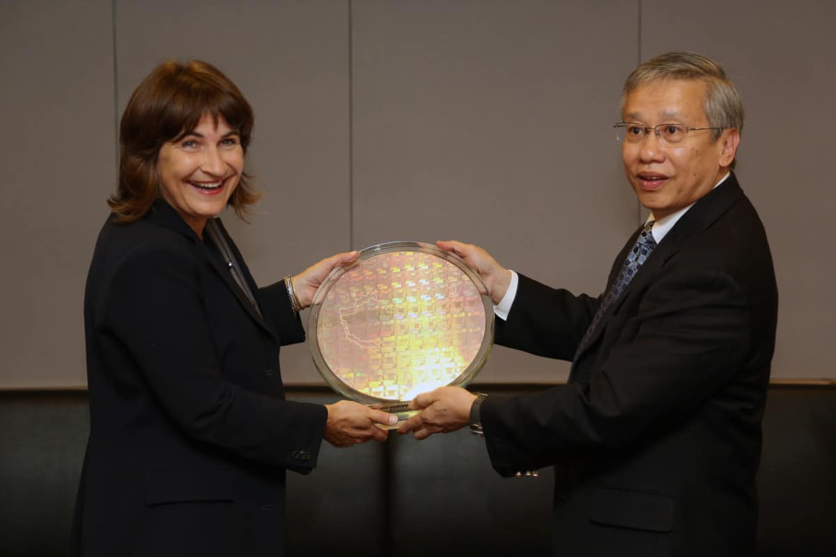
ASML, a Dutch technology company, had recently inked a deal with SMIC for one of its $120 million devices, which allows semiconductor manufacturers to make chips smaller, more powerful, and more energy efficient. ASML makes the world’s only extreme ultraviolet (EUV) lithography tools, and the chips they produce enable everything from smartphones to artificial intelligence (AI) devices and, eventually, advanced missiles. If SMIC secured one, China’s chip-making champion might finally join the industry leaders — Taiwan’s TSMC, America’s Intel and South Korea’s Samsung — all of whom use ASML’s machine.

Credit: Ministry of Foreign Affairs / Martijn Beekman, Global Entrepreneurship Summit
The U.S., however, is desperate to stop — or at least slow — China’s advancements in computer chips for both economic and national security reasons. China is currently about five to ten years behind the leading edge, while the U.S. dominates semiconductor manufacturing, capturing about 50 percent of the world’s market share in a $500 billion industry, one that Deloitte expects will grow to $1 trillion by 2030. In December, the U.S. placed SMIC on the Entity List, which restricts U.S. companies from exporting to a company without special approval, on the grounds that SMIC’s chips could find their way into military applications. EUV lithography, in particular, could help Beijing quickly upgrade its military, surveillance and AI technologies.
“Semiconductors underpin basically all advanced tech,” says Will Hunt, a research analyst at Georgetown’s Center for Security and Emerging Technology. “For China, that includes some problematic cases, such as using AI for military uses or developing hypersonic missiles. The possibilities for surveillance are also pretty concerning. Having leverage over these cases is really important.”
While the U.S. leads the semiconductor industry when it comes to chip design, sales, and most of the equipment for manufacturing, ASML is a notable exception. In 2017, the Dutch company, which was spun out of Phillips in the late 1980s, became the only company in the world to offer equipment to produce 5 nanometer chips — the smallest, most advanced available. When SMIC placed its order in 2018, the U.S. took notice. The deal, says Noah Barkin, managing editor for Rhodium Group’s China practice, represented something of a no-brainer for the Trump administration.
“It’s usually difficult to control some of these emerging and foundational technologies,” says Barkin, “but when Washington sees a big, expensive machine that is vital to China’s rise as a tech power, then it’s clear that it can do something to stop it.”
The U.S. began lobbying the Dutch government to stop the sale almost immediately after SMIC placed the order, one former senior official says. Several months later, in a move that has not been previously reported, Japan was brought into the discussion for assurances that they, too, would not sell next-generation lithography equipment to SMIC or any other Chinese company. (Canon is currently developing a competitor to EUV.) And finally, a few weeks after Pompeo spoke at the entrepreneurship summit, when the Netherlands Prime Minister Mark Rutte was visiting Washington, the U.S. again pressed for a halt to the sale: Deputy national security advisor Charles Kupperman presented Rutte with an intelligence report about what would happen if the Chinese were to acquire ASML’s technology.
At the time, the European Union was wary of China’s growing market and military power, but Barkin says its concerns were mostly focused on protecting European companies from Chinese acquisitions, not controlling exports. The Trump administration’s “very aggressive and much broader approach to export controls,” he says, “took the Dutch government and Europe by surprise.”
The latest ASML machine is just nuts… [EUV lithography] really is harder than getting to the moon.
Paul Triolo, practice head for geotechnology at Eurasia Group
According to James Andrew Lewis, director of the strategic technologies program at the Center for Strategic and International Studies, the ASML-SMIC deal represented a shift in the EU where security issues began to outweigh economic ones. “Left to their own devices,” he says, “the Dutch would have approved the license. The U.S. really had to go and lean on them largely on security grounds and say, ‘Do you think you can do this deal without creating risk both for your own economy and for Western security?’ ”
It can be difficult to appreciate how one machine could make the difference between Western primacy and Chinese ascendancy, but the technology at the center of ASML’s device is an engineering marvel. Research into EUV lithography began nearly 40 years ago, and once the basics were proven, it still took ASML more than 20 years and about 10 billion euros to get it to market. ASML persisted as, one by one, its competitors either missed their targets or threw in the towel. There’s the precision manufacturing processes, AI-based software that runs the tools, and the complexity of the tools themselves. The result is a combination of lasers, mirrors and molten tin that would make both Albert Einstein and Rube Goldberg proud.
“The latest ASML machine is just nuts,” says Paul Triolo, practice head for geotechnology at Eurasia Group. EUV lithography, he adds, “really is harder than getting to the moon.”
Which is why China wants it — desperately. Last year, Chinese companies made only about 6 percent of the chips used in the country. To make up the difference, China imported more than $300 billion worth of semiconductors — more than the country spends on foreign oil. Beijing has also added audacious goals for semiconductor self-sufficiency to its Made in China 2025 industrial program and committed to spending as much as $1.4 trillion to encourage its domestic industry.
“This whole planet is run by computer chips,” says Vivek Bakshi, president of consulting firm EUV Litho. “That’s why China wants in on it. Right now, they have to depend on everyone else.”
The pace of advancement in the semiconductor industry, however, is relentless, and while plenty of companies, including SMIC, have so far thrived using older tools to serve the lower end of the market, ASML’s EUV machines represent the future.
Credit: Ministerie van Buitenlandse Zaken (Ministry of Foreign Affairs), Creative Commons
THE MAGIC MACHINE
Lithography, in the simplest terms, is the process of creating transistors on silicon wafers — though even at the low end of the market, there is nothing simple about it.
The process starts with a thin slab of pure, clean silicon coated with a chemical known as a photoresist. The wafer is then inserted into a scanner, which shines light through a patterned mask. That light either hardens or softens the photoresist, and the softer parts are washed away. With the remaining pattern, engineers can do one of three things: they can etch channels into the exposed silicon; they can deposit metals into the photoresist’s gaps; or they can “dope” or impregnate the exposed silicon with another compound to change its electrical properties. Each adds features to the chip, and for complex chips, some steps are repeated dozens of times. Together, the channels, metal wires and doped silicon combine to form millions — or even billions — of transistors. The entire process, from pure silicon wafer to finished semiconductor, can take several months.
Because each additional transistor means more computing power, the industry has long been motivated to uphold Moore’s Law, which says the density of a chip’s transistors doubles every two years or so. Semiconductor companies have employed a range of clever hacks to create smaller features, but recently they hit a wall.
“To make them smaller, you have to think in terms of calligraphy,” says Bakshi. “You have to use a finer tipped pen to be able to draw the transistors. That means smaller wavelengths of light.”
Researchers in Japan and the United States began exploring EUV lithography — the finer tipped pen — in the 1980s, but it wasn’t obvious that it would work. Since air absorbs EUV, the lithography had to run in a vacuum, which made fine-tuning temperatures complicated (a fan is no good in a vacuum). Researchers also had to invent a new type of mirror to focus the EUV light since no lenses could be made transparent enough. And most problematic, they had to consistently generate sufficient amounts of EUV light.
ASML released a promotional video in 2009 showing off the soon-to-be-available EUV machines.
Scientists solved each of those problems one by one, but it fell to engineers to make the entire system commercially viable. If EUV scanners cost a fortune to run, no one would buy them.
“It was just such a daunting issue,” says Robert Maire, president of Semiconductor Advisors. “We’re up to a point where we use over 500 pieces of equipment in a $7–10 billion factory. The totality of the technology is huge. Back then, there was a question of whether there would ever be a financial payback.”
As different technologies were being tested in the 1990s, ASML hesitated to commit. The company had flirted with bankruptcy in the early 1990s and was still a third-rate player; in 1993, its market share was only 12 percent. By the late ’90s, however, the company had turned things around, and by the early 2000s its market share was 45 percent. It finally had the revenue to invest in EUV, while Nikon and Canon, the lithography industry leaders at the time, had been experimenting with EUV for years.
“ASML was very Johnny-come-lately,” says Harry Levinson, an independent consultant who previously led lithography research at GlobalFoundries. “They were very careful, studying the alternatives one by one and eliminating the ones they didn’t think would work. Once they concluded that EUV would work, they went after it with commitment.”
And just as ASML was doubling down, some of the bigger players, plagued by setbacks, were folding on EUV.
“There was only one technology around that appeared to enable the continuation of Moore’s law, and that was EUV,” says Chris Mack, chief technical officer of Fractilia, a lithography software company. “And there was only one company that was going to continue to invest, and that was ASML. So there became only one game in town.”
ASML used its customer base to finance its investment: Samsung, TSMC and Intel took stakes in the company in 2012 to fund EUV development — long before ASML was ready to ship production machines in 2017.
“If there had been alternatives, if the big semiconductor companies thought there was something else we could do besides EUV, I think things could have turned out differently,” says Mack.
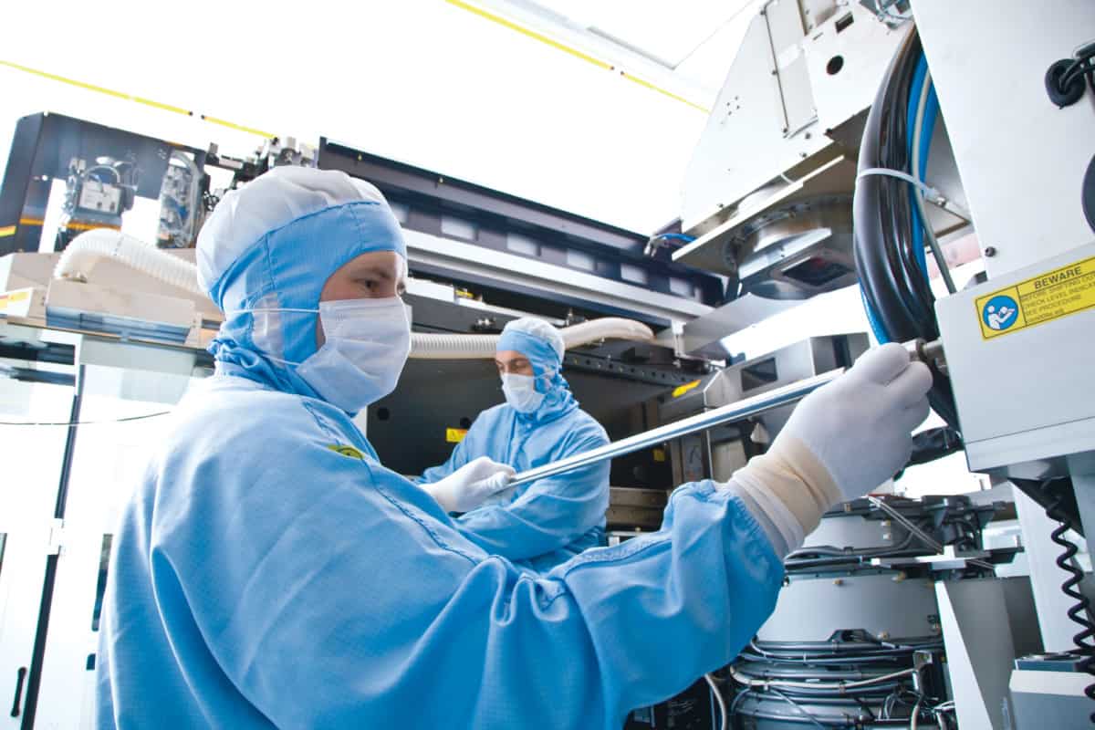
Indeed, had there been an alternative, EUV surely would have been abandoned. The process requires such precision and intricacy that it borders on magic. To produce 13.5 nanometer light and guide it to the wafer, ASML’s machine first melts tin into near-microscopic spheres and drops them into a vacuum chamber. Each speck of tin is tracked by ultrafast cameras so it can be zapped twice by powerful lasers. The first hit pancakes the droplet, flattening it so the next hit can impart more of the laser’s energy. The second strike vaporizes the tin into a ball of glowing plasma that emits EUV light. All of this happens 50,000 times per second. The emitted light is then focused and guided to the wafer by bouncing it off 11 specialty mirrors — one of which contains the desired pattern. These mirrors are made of more than 100 nanoscale layers of silicon and molybdenum, each polished to a precision measured in atoms. When the EUV light finally hits a silicon wafer, it can draw incredibly small features — every square millimeter can be covered with up to 230 million transistors.
“These EUV tools are engineering wonders,” says Mack. “You have to give ASML credit for the amazing feat they’ve achieved.”
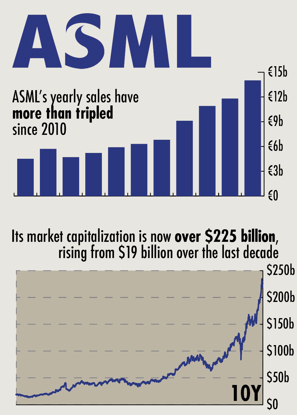
The broader industry seems to agree. Last year, ASML reported nearly $17 billion in revenue — more than double the 2016 figure, before its EUV machines were ready to ship. Its soaring stock price on Euronext Amsterdam and Nasdaq has made it the most valuable technology company in Europe, with a market capitalization of more than $225 billion. It shipped 31 EUV machines in 2020, and although none of them are headed for SMIC, China is still a growing market for ASML’s older technologies. In 2020, China accounted for 18 percent of ASML’s revenue, up from 12 percent the previous year.
In a statement to The Wire, ASML said: “ASML’s EUV systems are listed in the Wassenaar Arrangement which means that exporting EUV systems is only allowed if the exporter has an export license granted by the authorities of the exporting countries. A request for the export license for EUV to China is currently being processed by the Dutch government. Pending this process we cannot ship EUV to China. The decision is with the Dutch authorities and we are in contact with them.”
On the company’s recent earnings call, Peter Wennink, ASML’s chief executive, said: “We feel comfortable with the levels of potential growth expectations per business segment, but clearly see potential upside to these numbers when we can disregard any further impact of export control regulations resulting from the current geopolitical situation.” In other words, so long as ASML can ship older systems to China, the company’s China business seems poised to grow — even without EUV.
ASML currently has a backorder of at least 42 EUV machines anyways — a fact that Brigitte Dekker, a researcher with the Dutch think tank Clingendael, says proves the company isn’t significantly impacted by the recent export regulation. “Their machines are sold out. They had record high profits last year,” she says. “For ASML the regulation is not really an issue, but for China it is.”
THE TRUST CHAIN
It’s not clear when SMIC received the news. But in early November 2019, more than a year and a half after the company placed its order for the EUV scanner, word leaked out that the Dutch government hadn’t renewed ASML’s license to export the technology. The shipment wasn’t canceled, but it had been moved to “pending later notice.” To this day, SMIC has not received the machine.
It’s unlikely they ever will, a fact that SMIC seems to have tacitly acknowledged. By March 2020, SMIC began a public relations blitz, claiming that, by the end of the year, they would mass produce chips equivalent to TSMC’s previous generation, all without EUV.
“SMIC is going to pull out all the stops to try to squeeze the most out of its existing equipment,” says Triolo. “But it’s really hard to do. It’s really hard to get commercial yields out of that.”
In order to hack old techniques to increase the density of transistors, SMIC would have to use several masks — each of which adds time and expense — to achieve what EUV can do in just one. Each mask has to line up perfectly with the others; one micron of misalignment could ruin the entire wafer. If cost is no object, SMIC might try running the process over and over until they get a handful of chips that work. But, to Triolo’s point, that’s not exactly sustainable.
So what options is SMIC left with? The company currently lags about four generations behind industry leaders, and there’s a truism in semiconductor manufacturing that it’s almost impossible to skip generations, which are known in the industry as nodes. The problems at one node don’t disappear by skipping to the next one. In fact, they can become compounded in more advanced nodes, which means it might be better if SMIC ironed out their current issues before moving ahead.
Credit: ASML
“Yield is essential in all of this,” says Willy Shih, a professor at Harvard Business School. “The way you get that is you just tweak things, you do experiments. Over time, you learn how to make small improvements, but generally, you don’t get there by one big leap.”
Moreover, even if SMIC could land a few jumps, the company would eventually get to where TSMC was a couple of years ago, just before the Taiwanese company began using EUV. In other words, they’d still be lagging behind. In fact, experts say China has yet to even produce the previous generation of lithography tools, DUV immersion lithography scanners.2Analysts say on this tool, China may still be four or five years away from being commercial viable.
The other option would be to reverse engineer ASML’s equipment. But industry analysts say that’s a long shot. The complexity of the molten-tin light source is one challenge; double-tapping 50,000 tiny drops of tin with a laser every second is not your run-of-the-mill engineering problem. Another is the atomic-level precision mirrors, which are made by Germany’s Carl Zeiss, one of the most respected optical systems manufacturers in the world.
“Even if you were able to get your spies to steal everything Zeiss knows how to do, you still have to figure out how to make these things,” says Levinson.
And those are only two components of a system with over 100,000. There are the tracking cameras, the tools for quality control, the software used to design chips with EUV in mind — the list goes on.
“ASML has about 5,000 suppliers to produce that machine, many of whom are monopolists themselves — the sole suppliers in the world,” says John Lee, a senior analyst at the Mercator Institute for China Studies. “The range of things Chinese firms would need to replicate — many are built on decades of industry experience. That’s the nature of the choke points.”
Moreover, even if a reverse engineering effort was successful — or if Chinese researchers were to advance far enough on their own — SMIC would still have to figure out how to use it. The learning curve is not insignificant; it took Samsung and TSMC years of trial and error with EUV before they introduced it into their production lines. Intel is reportedly still struggling to do so.
“Trying to get something that actually works consistently is a huge challenge,” says Hunt, the Georgetown researcher. “You can share academic insights with reasonably high fidelity, but sharing deep engineering knowhow, and knowing how to put these different pieces of equipment together in a way that works, is really hard.”
ASML has about 5,000 suppliers to produce that machine, many of whom are monopolists themselves — the sole suppliers in the world… That’s the nature of the choke points.
John Lee, a senior analyst at the Mercator Institute for China Studies
The only option that makes sense, analysts say, is for SMIC to abandon advanced nodes for the time being and focus on less advanced chips that are still in high demand. That would leave the Communist Party in a tight spot, but even some prominent Chinese academics have second-guessed the self-sufficiency goals of Made in China 2025. “Are we doing the right thing today?” Wei Shaojun, a professor at Tsinghua University and board member of the China Semiconductor Industry Association, asked at a conference in November. “China has integrated into the global technology system and cannot go back.”
Indeed, the Chinese semiconductor effort is fighting headwinds: The overall trend in the industry is toward consolidation, not expansion. Because success at a new node requires herculean international research programs followed by enormous investments in facilities and machinery that is coordinated by world-class engineers with constant back-and-forth, a recent report from the Institut Montaigne, a Paris think tank, called the semiconductor value chain “a chain of trust.” So long as China remains outside that chain, it’s unlikely to be able to pull itself up.
That chain of trust is also very different from those involved in previous international export control regimes, like the 42-nation Wassenaar Arrangement. “The future of export controls is not Wassenaar, it’s these ad hoc, plurilateral export regimes.” says Tim Morrison, former senior director on the National Security Council for European affairs and now a senior fellow at the Hudson Institute in Washington.3Morrison was also senior director for Counterproliferation and biodefense, covering interagency control control processes. “This is where the Biden administration needs to go, a plurilateral agreement between the U.S., the Netherlands, Japan, South Korea, Germany, and Taiwan. That’s who you need — that’s all you need.”
Such agreements are likely to spread given China’s obvious ambitions. “The basic objective of preventing China from obtaining sensitive technology that they could use for military purposes is not going to go away,” says Barkin. Given the various choke points — EUV manufacturing chief among them — advanced chips are unlikely to be made in China anytime soon.

Tim De Chant is a journalist and editor and the founder of Future Proof, a publication covering climate and energy. He is a lecturer in MIT’s Graduate Program in Science Writing and has written for Wired, the Chicago Tribune, and NOVA Next, among others. @tdechant


